Kicad Labels
A common task for a transistor is switching a device on and off. Add a custom template with the same as the.gitignore template you want to use to the ~/templates directory on your system, and this generator will automatically use it.

[solved] Sheet label and hierarchical labels Schematic KiCad.info Forums
Kicad group information group information activity labels members epics 53 epics 53 list boards roadmap issues 1.9k issues 1.9k list boards milestones iterations merge requests 1.3k merge requests 1.3k security & compliance security & compliance security dashboard vulnerability report packages & registries packages & registries package registry

Kicad labels. Clearance is the minimum distance which needs to be maintained between the two tracks. 1843129 #1843129 select all missing from edit menu: Note that labels and power ports.
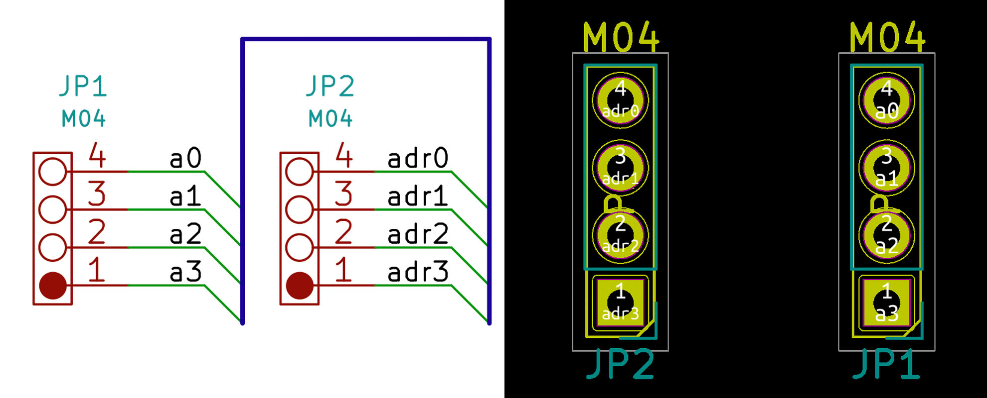
Labels and busses are local to the sheet that they are one. Library maintainer rules & guidelines. The target date is tentative and may be unrealistic.
Start up kicad and create a new project (file > new project > new project). Open source isa surely is an attractive title to geeks. Schematic capture, printed circuit board layout, gerber file viewer, solid model viewer, and much more.
The kicad development team released kicad 6 rc1 in november 2021, and 6.0 in december 2021. We use this milestone for bugs not targeted for 5.0. There are two configurations for a transistor switch:
Kicad 6 is full of improvements and new features, including a new file format, a refreshed user interface (with a new theme editor), a new schematic editing paradigm, field name templates and text variables, and. This defines a particular clearance. The first way to bring in labels is with global labels.
There are already some defined for you. It is important to go over these design rules in kicad. It features schematic capture, pcb layout and 3d viewer;
You can see over here, there are different nets. Name the project whatever you want. This can be a pain if you were planning on using kicad to just generate a spice netlist and running ngspice yourself, as you have to escape all net labels with the / by enclosing them in quotes (ngspice interprets / as the division operator).
We'll use labels for ease (a with a green line underneath on the right). Differentiating netnames when originating from local labels of multiple instances of hierarchical sheets: Kicad project information project information activity labels members repository repository files commits branches tags contributors graph compare locked files issues 1,414 issues 1,414 list boards service desk milestones iterations requirements merge requests 51 merge requests 51 ci/cd ci/cd pipelines jobs schedules test cases deployments
Generate is a command line tool and. The final step was to import the files into kicad and finish the board. For example, add a node.gitignore template to override the.gitignore template that's used when $ gen gitignore:node is run.
And you can see there is a default class available. It makes it easy to design schematics for electronic circuits and convert them into pcb designs. You could also get fancy by using laser printer foil or.
Low side and high side. Take some time and follow along and you'll be designing your own custom. It is unlimited in size, components and number of layers and has lots of the features of very expensive professional pcb layout software.
This is the largest release of kicad ever. Kicad supports an integrated design workflow in which a schematic and corresponding pcb are designed together, as well as standalone workflows for special uses. For our example board, we'll use pf0 for row0, pf1 for row1, pf4 for col0, and pf5 for col1:
For the purposes of this guide, i'll be calling it example. Kicad automatically shares power labels, such as vcc and gnd., throughout a schematic project. If this price is not low enough for you, here is a sbc based on d1s, the.
Kicad will append a / to the front of all manually added net labels. Kicad will handle that part once you define this minimum clearance. Multiple sheet schematics in kicad.
Kicad is a full feature electronics development application for the design and manufacture of electronics that runs natively on windows, osx, and linux. The box looks great and this seems easier than using, say, waterslide paper to create labels. But kicad offers two ways to bring nodes into a hierarchy of sheets.
The software used is kicad 5.0. Widgets available in tkinter include (but are not limited to) button, canvas, check button, combo box, frames, labels, progress bars, scroll bars, and text.

How to change netnames? Layout KiCad.info Forums

Net Labels not connecting? Schematic KiCad.info Forums

Kicad Global Label Vs Net Label Circuit Boards

Kicad Global Label Vs Net Label Circuit Boards
Kicad Global Label PCB Designs

How to change netnames? Layout KiCad.info Forums

Wrong placement of reference and value labels Schematic KiCad.info Forums

[Mac OS X] ground pin and Bus to wire labels Schematic KiCad.info Forums
Create nets and labels Kicad Like a Pro


Add text labels Kicad Like a Pro

Kicad Global Label PCB Designs

Hierarchical Labels with Repilcate Layout External Plugins KiCad.info Forums

Power plane for global label Layout KiCad.info Forums
Kicad Global Label PCB Designs

Labels for inverted signals Schematic KiCad.info Forums

[Mac OS X] ground pin and Bus to wire labels Schematic KiCad.info Forums

KiCAD Hierarchical Labels General Electronics The Contextual Electronics Forums

KiCad 5 (Part 17) Hierarchical Labels & Pins YouTube
Labels for inverted signals Schematic KiCad.info Forums